The design process to develop our electronics projects uses the same baseline as the design process for our mechanical projects, to learn more about our design process please refer to our Mechanical design process page
PCB footprint is determined in the early phase of the project, to our experience PCB size (this can be multiple PCB’s as well) is strongly related to physical form factor of the product and is therefor constraint. How tight this constraint is, differ from product to product. However pre-determining PCB footprint has been proven to be a good habit to start with in electronics designs and is therefore embedded in our way of working. Often it's challenging to increase PCB size while there are multiple design techniques to reduce “function block” area claims within the PCB footprint, so optimisation of area claims is first before resizing the PCB(‘s). Optimisation techniques for area claims are,
- Schematic's architecture
- Component size / packaging
- Number of layers used in the PCB
- PCB stacking (addition of PCB’s), to us this falls into the “PCB resizing” category
Area claims are the individual area's on a PCB that are required / reserved for each function block. The sum of the area claims is the total electrical solution on the complete PCB(‘s). By claiming area's on the PCB(‘s) gives focus on important aspects of electronics design, like
- Interaction / interfacing between function blocks
- External interfacing to and from function blocks (e.g. connector locations, other PCB’s)
- Amount of components used to build the function blocks
- Pin layout on the MCU
- Options for energy storage (battery’s, capacitors)
- EMC reduction (location of high speed traces, power planes, oscillator placement)
Function blocks are (preferably) isolated functions on the PCB. Defining functions can be, at times, challenging however when this is done properly it will have many advantages, knowing
- Test definition and execution
- Solving issue and function optimisation
- Alternatives studies
- Reuse of proven function blocks in other projects
- Growing knowledge on reliability of the function block and therewith, in case of reuse, ‘first time’ right confidence in other projects including decrease in required tests
- Reduction of EMC risk compared to new function blocks
In general all function blocks that we design, will be build in LT spice. Using LT Spice makes it possible to test and optimise the function block already before it is actually built. It also allows us to do (some) variation study, for instance by changing the values of the components that built-up the function block. When the function block gives satisfactory results, we use LT Spice also in (pre-)determining the test protocols for the function block. Having a draft version of the test protocol ready is important for the next step, the breadboard
The Breadboard is an indispensable step in our electrical design process. All new function block designs will be tested on the breadboard
before we order any (prototype) PCB and preferably before we even start PCB lay-out. The flexibility of swapping, replacing and adding components to the
circuit is unsurpassed on a breadboard. Tweaking the performance of the function block and the resulting gain on the finest details of understanding the
function block has turned out to be a huge benefit. In some cases we will even go a step further and design a dedicated function block test PCB’s as a
intermediate step in the process towards the final PCB
The foundation of designing a dedicated function block lies in (some) following reasons
- Breadboard connections are not perfect
- Optimisation of component placement with respect to each other
- Use of actual components instead of “breadboard” components
- Adding “tweaking” parts (e.g. potentiometers) for performance optimisation
- Pre EMC studies with spectrum analyser
- Design of test points on the PCB for improving measurements
The use of microcontrollers in electronics designs is mostly the case. The microcontrollers we use are generally the PIC24 and PIC32 series from Microchip. Next to the MCU’s from Microchip we also use Arduino and Raspberry PI as platforms to interact with the function blocks
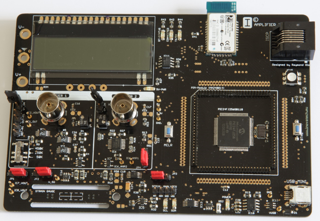
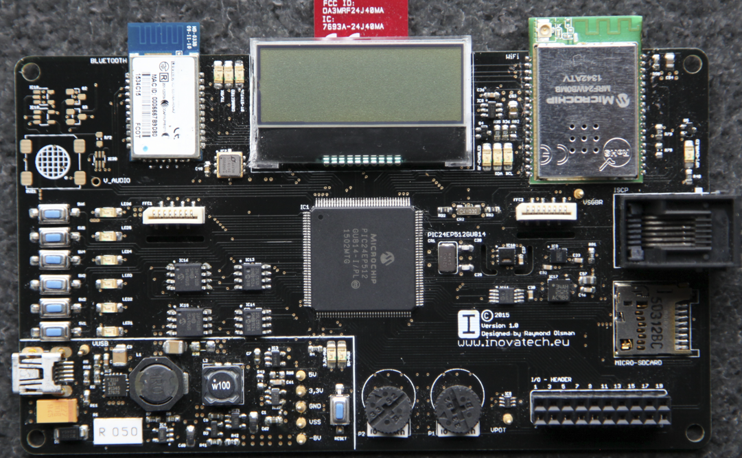
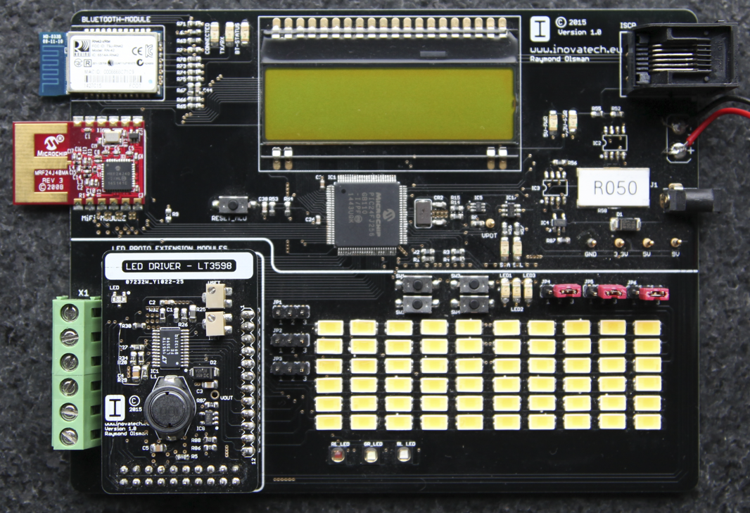
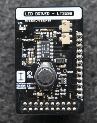
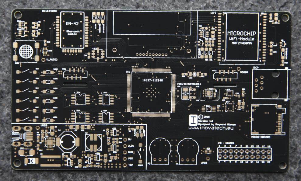
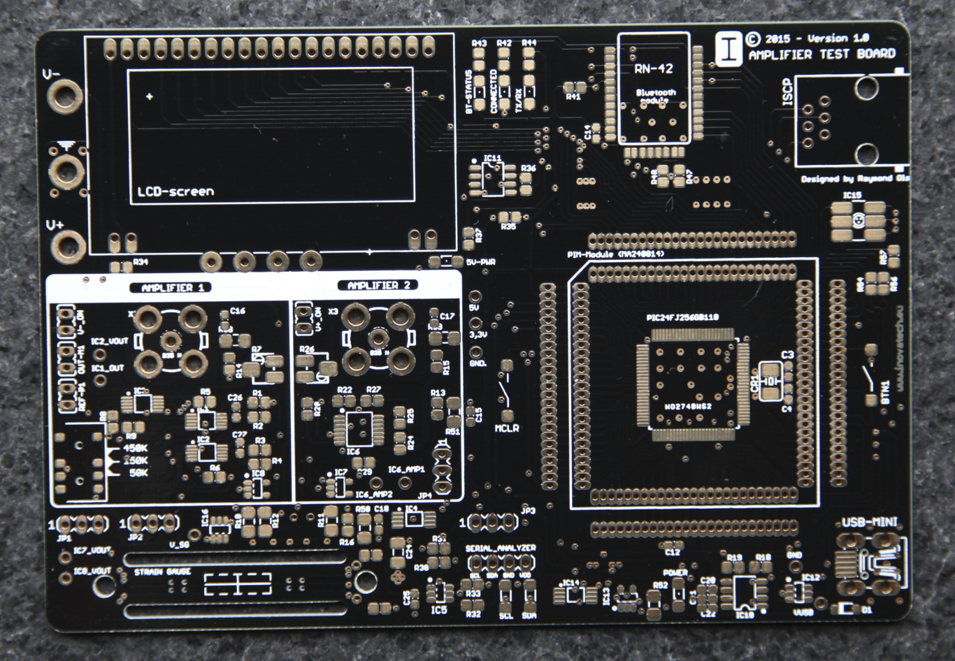
After passing the LT spice and breadboard phase it is time to lay-out the components of the function blocks op the PCB. We favour tidiness and thought through component placement,
out might set is that a board must have some sort of aesthetics to meet. How we think about that is shown in the PCB pictures below, to our opinion these boards to meet the aesthetics
of good looking PCBA’s. It's due to our view on aesthetics that our boards are standard in the colour black on gold, on customer request we can change that of course
We design our electrical schematics and PCB lay-outs in Eagle. It’s due to our way of working that the schematics are designed in functional blocks as well, rather than one big schematic.
This allows us to easily re-use those function blocks in other projects. With regards to PCB lay-out our experience is that this is unique for each project, with the remark of reusing
function blocks where the base is that the routing is fixed this of course within reasons
As mentioned in PCB footprint section, our approach for PCB lay-out is to up-front determine the functional blocks areas and resulting main components of these function blocks on the PCB.
When the general component placing is done it is possible to start the pin lay-out of the MCU’s and other components that have flexibility in their pin out. In a properly organized
pin-layout the amount of "trace" cross overs is minimized. In our view the determination of pin connections, especially with MCU's is key to have a 'clean' and 'aesthetically pleasing'
layout on the PCB
When the PCB’s come in from our supplier, we execute the following steps
- Visual inspection of the PCB
- Trace resistance measurements
- Check (critical) traces from component to component
- Based on our test protocol component placement
- Intermediate tests, for example first built the power supply and execute the test protocol for this function block
- Final PCB test